“`html

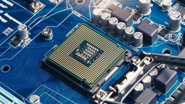
Researchers have devised a “back-end memory transistor” that combines a processing unit (the transistor) with a storage unit.(Image credit: Christine Daniloff, MIT; iStock)ShareShare by:
- Copy link
- X
Share this article 0Join the conversationFollow usAdd us as a preferred source on GoogleNewsletterSubscribe to our newsletter
MIT engineers suggest that arranging circuit parts one atop the other may present a solution for designing more power-saving artificial intelligence (AI) chips. The logic and memory segments, which conduct calculations and retain information respectively, can exchange information more conveniently through direct contact, rather than when physically separated.
The team originated a “memory transistor,” encompassing a logic component capable of carrying out operations (the transistor) and a storage segment. This diminutive device possesses relatively few electrical flaws, indicating enhanced speed and reduced energy consumption, according to findings shared in a pair of studies presented on December 9 and 10 during the International Electron Devices Meeting held in San Francisco.
You may like
-
China solves ‘century-old problem’ with new analog chip that is 1,000 times faster than high-end Nvidia GPUs
-

Scientists say they’ve eliminated a major AI bottleneck — now they can process calculations ‘at the speed of light’
-

Scientists create world’s first microwave-powered computer chip — it’s much faster and consumes less power than conventional CPUs
A single interaction with ChatGPT can produce sufficient warmth to necessitate a water bottle’s worth of cooling. However, the majority of energy linked with AI is expended conveying data between components rather than conducting computations. Even a modest energy conservation at the chip level could yield significant results, the scientists believe.
“We must lessen the degree of energy utilized for AI and other data-focused computation moving forward as it’s simply untenable,” stated Yanjie Shao, the study’s lead author and a postdoctoral researcher at MIT, via a press release. “To continue advancing, we’ll require novel technology like this integration platform.”
Stacking conserves energy — yet poses difficulties
Modern chips incorporate logic circuits fabricated from transistors, which act as on/off mechanisms governing current flow. These transistors merge to denote binary 1s and 0s, enabling information processing by chips. Additionally, they feature memory circuits, containing transistors along with other substances capable of data storage.
Logic and storage circuits are generally maintained separately, necessitating data transfer through wires and interconnections, resulting in energy wastage. Although arranging the active parts vertically may appear to be an intuitive solution, the challenge lies in executing it without inducing damage. For instance, deposition, the regulated creation of extremely thin layers forming these components, must occur at lower temperatures because certain transistors cannot endure elevated heat.
To resolve this issue, the researchers constructed their logic transistor employing an active channel layer (the zone facilitating electricity flow) composed of indium oxide. Significantly, the substance can be placed in a two-nanometer layer at approximately 302 degrees Fahrenheit (150 degrees Celsius). This temperature is adequately low to avoid impacting other transistors.
Beyond the indium oxide transistor, the scientists vertically assembled a memory element — a 10-nanometer layer of ferroelectric hafnium-zirconium-oxide — empowering the device to both retain and manipulate data. The subsequent memory transistor can activate or deactivate in a mere 10 nanoseconds, running at less than 1.8 volts. The switching velocities of typical ferroelectric memory transistors generally rank significantly lower and demand voltages ranging from 3 to 4V.
The memory transistor attains even greater efficiency through construction on the chip’s “back-end,” housing the wires and metal connections that link the front-end’s active components. According to Shao, this process significantly enhances the chip’s integration density.
RELATED STORIES
—China solves ‘century-old problem’ with new analog chip that is 1,000 times faster than high-end Nvidia GPUs
—World’s first light-powered neural processing units (NPUs) could massively reduce energy consumption in AI data centers
—Scientists create world’s first microwave-powered computer chip — it’s much faster and consumes less power than conventional CPUs
For the purposes of the two studies, the memory transistor existed solely on a chip-like framework instead of a functional circuit. The team anticipates refining the transistor’s capabilities, enabling its initial integration into a distinct circuit, followed by incorporation into more extensive electronic systems.
“Presently, we are capable of erecting a platform of adaptable electronics on a chip’s back end, facilitating elevated energy efficiency and diverse functionalities in extremely compact devices,” Shao stated. “We possess a favorable device architecture and material to proceed with; however, continued innovation remains vital for unveiling the ultimate performance capabilities.”

Fiona Jackson
Fiona Jackson acts as an independent writer and editor, with a primary focus on science and technology. She has functioned as a news writer within the science division at MailOnline, and has also reported on technology news for TechRepublic, eWEEK, and TechHQ.
Fiona gained vital experience penning human interest narratives for global news sources at the SWNS press agency. She possesses a Chemistry Master’s degree, an NCTJ Diploma, and shares her residence in Bristol, UK, with a cocker spaniel called Sully.
Show More Comments
You must confirm your public display name before commenting
Please logout and then login again, you will then be prompted to enter your display name.
LogoutRead more

Scientists say they’ve eliminated a major AI bottleneck — now they can process calculations ‘at the speed of light’

‘Rainbow-on-a-chip’ could help keep AI energy demands in check — and it was created by accident

‘Putting the servers in orbit is a stupid idea’: Could data centers in space help avoid an AI energy crisis? Experts are torn.

New semiconductor could allow classical and quantum computing on the same chip, thanks to superconductivity breakthrough
Breakthrough 3D wiring architecture enables 10,000-qubit quantum processors

Scientists build ‘most accurate’ quantum computing chip ever thanks to new silicon-based computing architecture
Latest in Computing

Scientists build ‘most accurate’ quantum computing chip ever thanks to new silicon-based computing architecture
This new DNA storage system can fit 10 billion songs in a liter of liquid — but challenges remain for the unusual storage format

Record-breaking feat means information lasts 15 times longer in new kind of quantum processor than those used by Google and IBM

New ‘DNA cassette tape’ can store up to 1.5 million times more data than a smartphone — and the data can last 20,000 years if frozen