in News
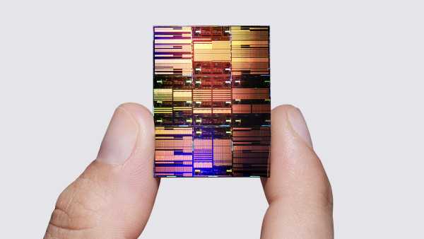
Quantum chips are notoriously “noisy,” with interference disrupting calculations, but scientists want to introduce more errors to learn how we protect against them.(Image credit: IBM)
- Facebook
- X
- Reddit
- Pinterest
- Flipboard
Share this article 0Join the conversationFollow usAdd us as a preferred source on GoogleSubscribe to our newsletter
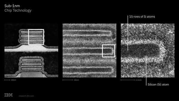
For the first time, researchers have developed computer chips featuring transistors smaller than 1 nanometer. The new “NanoStack” architecture enabling this breakthrough could potentially yield transistors as tiny as 0.1 nm in the future, according to the scientists.
The newly developed 0.7 nm transistors are considerably smaller than those found in conventional 2 nm semiconductor chips utilized in supercomputers, AI systems, and advanced graphics processing units (GPUs). While the size designation doesn’t always precisely reflect the transistor dimensions, it generally indicates their performance capabilities.
In essence, smaller transistors and their associated components allow for a higher density on a chip. For instance, a typical 2 nm chip design can accommodate approximately 50 billion transistors within a space the size of a human fingernail.
The transistors on the new chip are so minute they are measured in “angstroms,” a unit of length typically used for atoms, rather than nanometers. The initial batch of these chips is anticipated to be produced with transistors measuring just 7 angstroms, which equates to 0.7 nanometers or approximately the width of a glucose molecule.
At this scale, engineers can fit close to 100 billion transistors into an area the size of a fingernail, nearly doubling the capacity of the current 2 nm platform.
Stacking and staggering
The researchers accomplished this by employing a novel approach termed “nanostacking,” which they first detailed in a study presented at the peer-reviewed 2025 Symposium on VLSI Technology and Circuits and subsequently uploaded to the IEEE Xplore server in July 2025. This method permits engineers to vertically arrange the nanosheets that constitute the previous generation of 2 nm computer chips.
The established technology for all conventional circuits, known as complementary metal-oxide-semiconductor (CMOS), requires exceptionally high temperatures during its fabrication process. As transistors shrink, they also encounter issues like “charge trapping,” where electrons or holes become fixed due to imperfections or contaminants, and “gate leakage,” a form of static power dissipation.
These challenges have impeded efforts to reduce transistor dimensions below 2 nm, thereby enhancing the performance and efficiency of computer chips beyond current benchmarks. However, IBM’s three-dimensional stacked architecture is designed to mitigate some of these difficulties, according to the scientists.
“NanoStack involves stacking nanosheet transistors on top of one another, achieved not through a simple, monolithic lithography and etching process,” explained Huiming Bu, vice president for IBM semiconductors global R&D and Albany operations, during a press briefing.
“What we do here is actually stack the device. I refer to it as stacking, but also staggering. It’s stacked vertically, allowing the front and back of each transistor to be independently contacted for signals and power. The assembly of these transistors is accomplished through single dielectric bonding, which represents a significant innovation we have developed.”
(Image credit: IBM)
IBM representatives indicated during the briefing that the new technology offers up to a 50% boost in performance while consuming 70% less energy compared to the 2 nm platform, and it is expected to fully supersede this technology within the next five years.
The researchers suggest that this advancement could profoundly impact the computing industry, bringing transformative changes to the fields of artificial intelligence (AI) and quantum computing.
One of the immediate practical advantages could be the creation of superior static random access memory (SRAM) chips, which are integral to various computing applications, including CPU caching, networking, and essential components in devices like pacemakers and automotive sensors.
SRAM also plays a crucial role in AI processing. Its proximity to processing cores, unlike other RAM modules often situated as separate units, accelerates data transfer within systems, thereby reducing performance bottlenecks.
During the press briefing, IBM representatives shared that they demonstrated a 40% improvement in SRAM memory scaling compared to the 2 nm platform. This development is anticipated to significantly benefit AI workflows, which necessitate considerably higher bandwidth and efficiency.
The future of computing
“We have truly entered a realm where semiconductor manufacturing feels almost magical,” Huiming Bu commented on the design process. “Consider the structure we are constructing here. We are depositing layers atom by atom, building up the structure precisely, atom by atom.”
IBM representatives stated that the nanostacking method represents not just an incremental improvement but a paradigm shift that will eventually enable foundries to scale these chips from 0.7 nm transistors down to a single angstrom, or 0.1 nm, thereby extending the viability of Moore’s Law.
Shrinking the transistor nodes on these chips will facilitate more powerful processing capabilities, they noted, owing to a nearly twofold increase in transistor density. Simultaneously, the stacked and staggered design substantially curtails energy demands. Huiming Bu remarked that while everyone desires enhanced performance, few are willing to bear the increased power consumption costs.
“It will supplant nanosheet technology as the current mainstream platform at leading foundries, applicable to both CPUs and GPUs,” he added. “We anticipate this transition to occur around the 7-angstrom mark. Consequently, within a decade, this will become another mainstream platform that we have pioneered. This signifies the next major technological leap.”
Related stories
- Microsoft’s innovation might reduce quantum computer errors by a factor of 1,000
- The quantum internet is progressing thanks to a new chip that aids in transmitting quantum signals over actual fiber-optic cables
- Scientists utilized an IBM quantum computer to train an AI model, which then correctly answered questions that the original model could not
The findings from the 2025 study indicate that the chipset not only offers significantly enhanced performance with reduced energy consumption but also presents a potential pathway to mitigate the thermal effects of high-power computing on hardware.
These advancements may also influence quantum computing, according to IBM representatives, by improving the classical systems that will work in conjunction with quantum computers as the technology matures.
“For quantum computing, we require substantial classical computational resources,” stated Jay Gambetta, IBM’s director of research, during the press conference. “We need to develop decoders, controllers for decoders, and accelerators. We are currently developing these classical components using the 2 nm platform. Enhancing the platform and utilizing more efficient, powerful chipsets will only accelerate the development of the necessary classical compute infrastructure that complements quantum systems.”
TOPICS
Sourse: www.livescience.com